Login
Sign Up
Member Area
Login
Sign Up
English
Afrikaans formal
Afrikaans informal
Arabic
Azerbaijan
Brazilian
Bulgarian
Catalan
Chinese simplified
Chinese traditional
Croatian
Czech
Danish
Dutch
English
Estonian
Finnish
French
Georgian
German
Greek
Hebrew
Hungarian
Icelandic
Indonesian
Italian
Japanese
Latvian
Lithuanian
Malaysian
Norwegian
Persian
Polish
Portuguese
Romanian
Russian
Serbian
Slovakian
Slovenian
Spanish
Swedish
Thai
Turkish
Ukrainian
Vietnamese
Toggle navigation
VideotonStock
Your Shopping Cart is empty.
Files
Stock
Photo
Video
Special offer
Collections
Packages
Lightboxes
Licenses
Royalty free
Rights managed
Creative
Editorial
Items
Most downloaded
Featured
Most popular
New
Free
Categories
Browse categories
Site info
Site info
About
Support
Privacy Policy
Privacy Policy
FAQ
Contact Us
Contact Us
Terms and Conditions
Buyer Agreement
Seller Agreement
Customers
Users
Credits
Photographers
Boby Richards
0
Boby Richards
0
Videoton1
286
Search
Keywords:
Creator ID:
Type:
Photo
Illustration
Vector
Video
Template
3d
Categories:
Animals
Buildings and Architecture
Business
Drinks
The Environment
States of Mind
Food
Graphic Resources
Hobbies and Leisure
Industry
Landscapes
Lifestyle
People
Plants and Flowers
Culture and Religion
Science
Social Issues
Sports
Technology
Transport
Travel
News
Entertainment
Sport News
Languages:
Brazilan Portuguese - Brazil
English - Canada
French - Canada
Spanish - Mexico
English - United States
English - Belgium
French - Belgium
Dutch - Belgium
Czech - Czech Republic
English - Cyprus
Danish - Danmark
German - Germany
English - Estonia
Spanish - Spain
French - France
French - Marocco
English - Greece
English - Ireland
Italian - Italia
English - Latvia
English - Lithuania
German - Luxembourg
English - Luxembourg
French - Luxembourg
English - Hungary
English - Malta
Dutch - Nederlands
Bokmal Norwegian - Norway
German - Austria
Polish - Poland
Portuguese - Portugal
English - Romania
German - Switzerland
English - Slovenia
Slovakian - Slovakia
French - Switzerland
English - Finland
Swedish- Sweden
Italian - Switzerland
English - United Kingdom
English - Bulgaria
English - Australia
Japanese - Japan
Korean - South Korea
English - New Zealand
Russian - Russia
English - Ukrain
English - Thailand
Orientation:
All
Horizontal
Vertical
square
Color:
Model property release:
All
Yes
No
Duration Video:
All
Up to 10 seconds
Up to 20 seconds
Longer than 30 seconds
Results
(0)
Site
Getty/iStock
Bigstockphoto
Pixabay
Adobe Stock
Relevance
New
Most popular
Most downloaded
Undiscovered
12
24
36
48
96
Auto paging
Menu
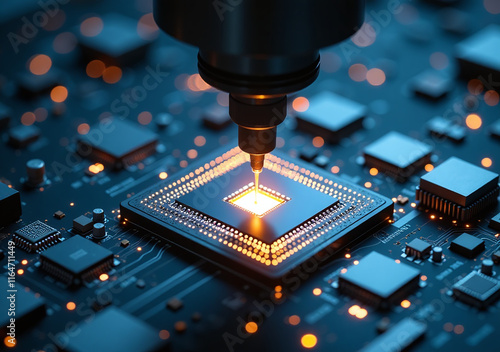
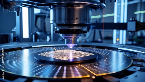
A high-resolution close-up of a photolithography process in chip manufacturing.
Nanolithography Icon
Engineers are enhancing photolithography techniques for smaller transistor nodes.
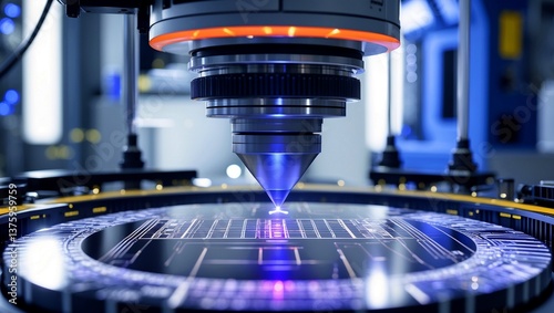
Advanced photolithography process used in semiconductor manufacturing .
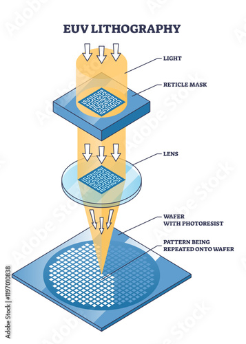
EUV lithography diagram shows light, reticle mask, and wafer interaction, transparent background.
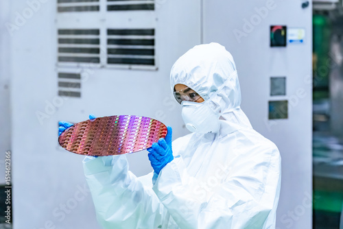
半導体工場でシリコンウエハーを検査する防護服を着た女性作業員
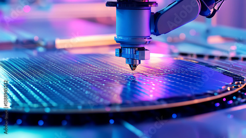
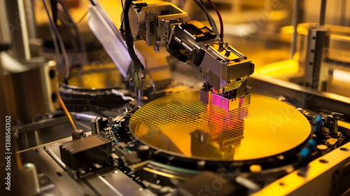
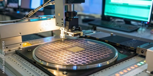
A robotic arm in a modern semiconductor fabrication plant, surrounded by wafers, photolithography equipment
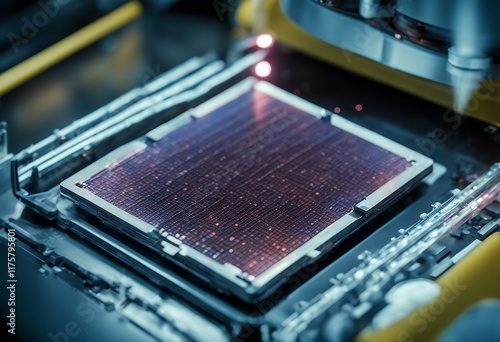
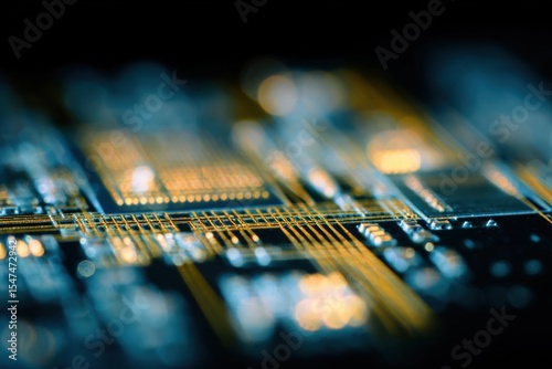
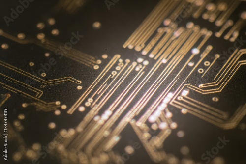
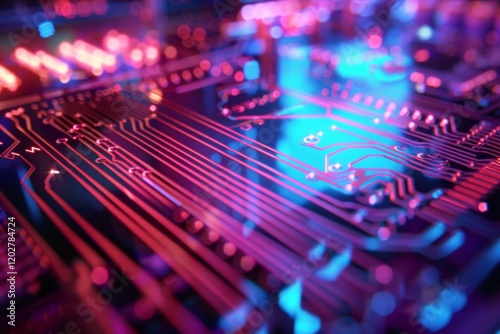
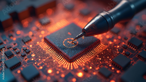
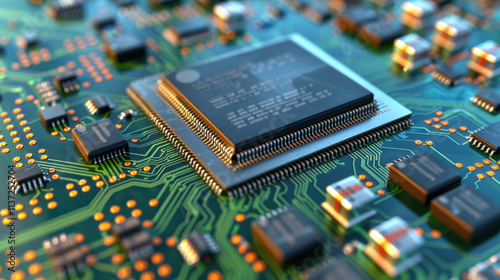
Transistor unit mounted on a motherboard with detailed gold circuits
Precision equipment handles silicon wafers in a semiconductor manufacturing facility, showcasing intricate processes under vibrant lighting conditions.
A robotic arm in a semiconductor cleanroom, placing silicon wafers into a photolithography machine, sterile white environment
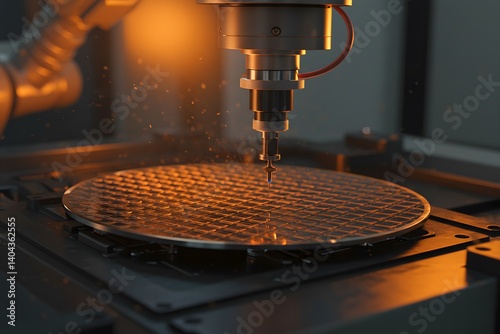
photolithography process in semiconductor
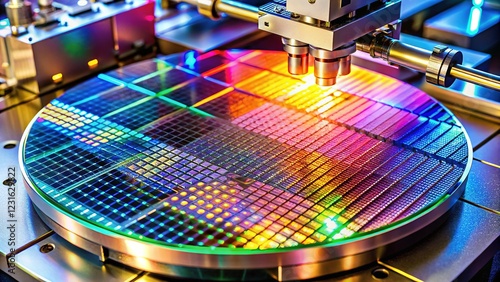
semiconductor manufacturing occurs complex machines producing computer chips using silicon wafers photolithography
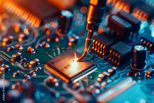
Close-up of Advanced Computer Chip illuminated with Red Light in Industrial Environment. Microchip on Conveyor Line during Production and Packaging Process on Semiconductor Fab
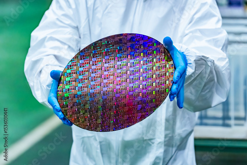
Semiconductor wafer and photomask used in industry for production of microchips and integrated circuits in clean environment
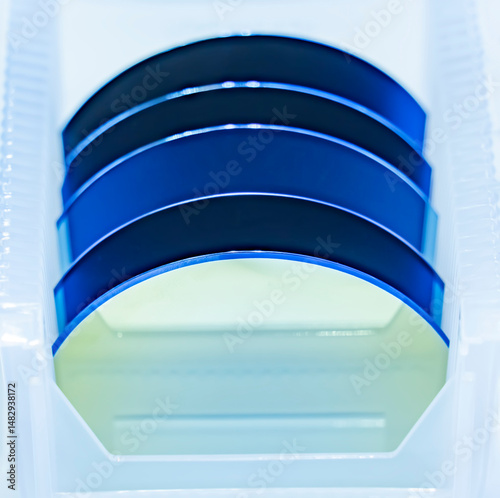
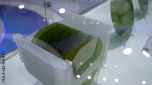
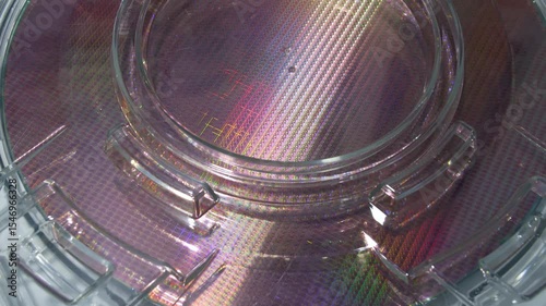
patterned silicon wafers in a universal pod. Electronic circuit designs have been built onto the wafers using micromaching including photolithography
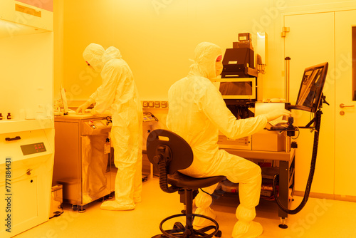
A semiconductor wafer fabrication clean room with technicians in full protective gear, advanced machinery etching micro-circuits onto silicon wafers, and precision instruments ensuring accuracy
Computer Chip illuminated with Blue Light in Industrial Environment. Microchip on Conveyor Line during Production and Packaging Process on Semiconductor Fab. Processor at Engineering Laboratory
patterned silicon wafers in a universal pod. Electronic circuit designs have been built onto the wafers using micromaching including photolithography
Semiconductor Chip Etching Process in a Manufacturing Facility. Concept Semiconductor Manufacturing, Chip Etching, Clean Room Procedures, Chemical Safety Practices, Production Efficiency
Close-up of semiconductor wafer under inspection in a fabrication facility, highlighting precision and quality control. Close-up of a semiconductor wafer being processed by a precision robotic arm
Modern Integrated Circuit Design | Close-Up of Advanced Microchip Technology
Nanolithography Icon
Engineers are enhancing photolithography techniques for smaller transistor nodes.
Euv lithography process in advanced ai chip manufacturing
EUV lithography diagram shows light, reticle mask, and wafer interaction. Outline diagram
半導体工場でシリコンウエハーを検査する防護服を着た女性作業員
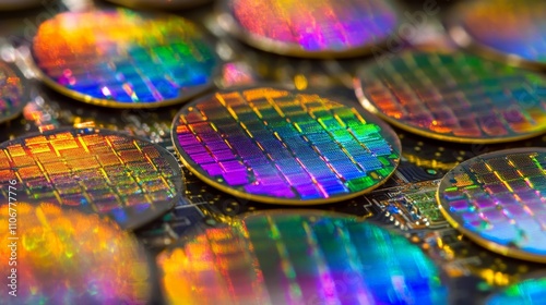
Stacked colorful silicon wafers with intricate holographic reflections and etched microchip patterns, symbolizing advanced semiconductor manufacturing and cutting edge technology
production chip computer machine photolithography complex process wafer silicon
A mechanical arm in an advanced chip manufacturing plant, surrounded by silicon wafers, photolithography machines
A robotic arm in a semiconductor cleanroom, placing silicon wafers into a photolithography machine, sterile white environment
photolithography process in semiconductor
complex computer chip production involves photolithography silicon wafers manufacturing process fab foundry facility every
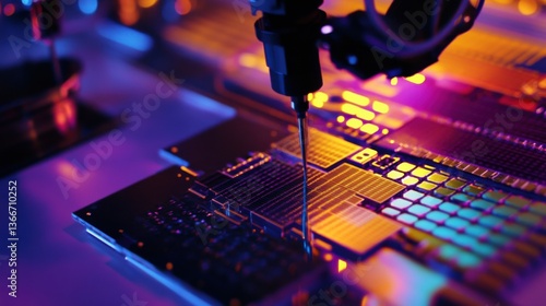
A medium closeup of a cleanroom environment focusing on a photolithography stepper. The image captures the complex optics and exposure system illustrating the layered lens assemblies
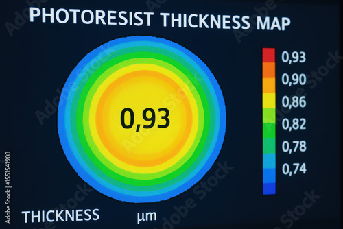
Photolithography process in semiconductor industry production with photresist thickness map precise measurement for quality control
patterned silicon wafers in a universal pod. Electronic circuit designs have been built onto the wafers using micromaching including photolithography
Cleanroom Scientist Examining Rainbow Silicon Wafer Under Blue Light
3D rendering of cyberpunk AI. Circuit board. Technology background. Central Computer Processors CPU and GPU concept. Motherboard digital chip
patterned silicon wafers in a universal pod. Electronic circuit designs have been built onto the wafers using micromaching including photolithography
A high-resolution close-up of a photolithography process in chip manufacturing.
semiconductor process with laser beams creating intricate microchip patterns on silicon wafers
Close-Up View of Semiconductor Chip Under Microscope
High-Tech Semiconductor Lab Technician with Wafer
Engineers are enhancing photolithography techniques for smaller transistor nodes.
Innovative photolithography techniques for silicon wafer production technology lab digital imaging
Advanced semiconductor manufacturing process in a clean room environment with intricate machinery and equipment
半導体工場でシリコンウエハーを検査する防護服を着た女性作業員
A silicon wafer undergoes production at an advanced semiconductor foundry specializing in microchip manufacturing
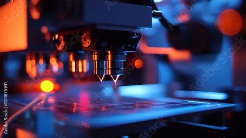
A microchip wafer undergoes ultraviolet light exposure, essential for photolithography in semiconductor manufacturing. This process ensures precise pattern transfer on the wafer surface.
monochrome
A robotic arm in a semiconductor cleanroom, placing silicon wafers into a photolithography machine, sterile white environment
photolithography process in semiconductor
photolithography process creates complex patterns silicon wafers used semiconductor
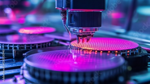
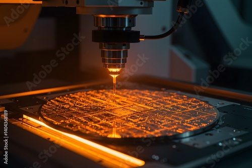
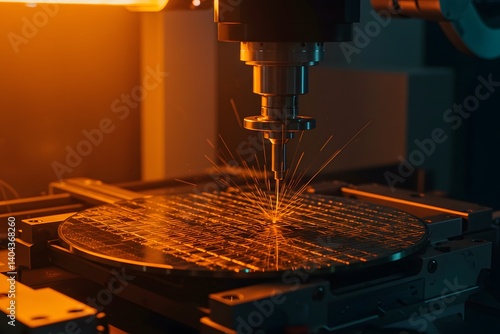
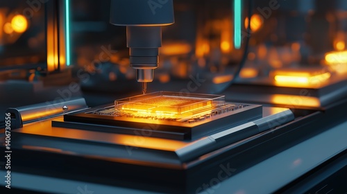
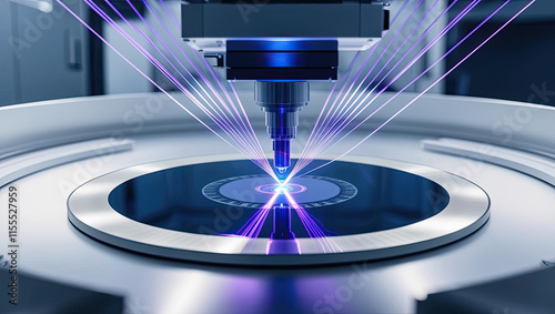
A photolithography machine in action projecting light patterns onto a silicon wafer with precision equipment and control panels visible in the background.
Close-up of a semiconductor wafer being processed by a precision robotic arm during the manufacturing process, Close-up of semiconductor wafer under inspection in a fabrication facility
precision and quality control. Close-up of a semiconductor wafer being processed by a precision robotic arm during the manufacturing process, Close-up of semiconductor wafer under
Semiconductor Manufacturing: Front View of Silicon Wafer in Photolithography Process
Wafer cassette loaded into a photolithography stepper in a clean room
patterned silicon wafers in a universal pod. Electronic circuit designs have been built onto the wafers using micromaching including photolithography
Photolithography machine assembly
Nanolithography Icon
Close-Up View of Semiconductor Chip Under Microscope
Close-up of semiconductor wafer under inspection in a fabrication facility, Close-up of a semiconductor wafer being processed by a precision robotic arm during the manufacturing process,
Employees are calibrating photolithography machines to maintain accuracy in chip designs.
Stacked wafers symbolize semiconductor fabrication layers.
Silicon Wafer Production at Semiconductor Foundry Illuminated by Light
Photolithography lab
factory, holding, hand, semiconductor, silicon wafer, pattern, circuit, substrate, manufacturing, deposition, photomask, worker, cleaning, processing, resist coating, photolithography, resist, process
Creating silicon wafers
Microchip fabrication in cleanroom environment with photolithography machine and laser etching tools. Semiconductor manufacturing process showcasing nanotechnology and microscopic circuit patterns
A robotic arm in an advanced semiconductor fabrication lab, assembling photolithography equipment for advanced microchips with AI accuracy, Electronics-tech style
PFAS products black line icons set for digital and print projects.PFAS product
photolithography process in semiconductor
A microchip wafer is being processed with ultraviolet light, essential for photolithography in semiconductor manufacturing. Precision equipment plays a vital role in forming complex circuits.
Semiconductor Fabrication Plant: Specializes in creating microchips for a wide range of electronics and computing applications, enabling faster, smarter technology for modern society.
A photolithography machine in action projecting light patterns onto a silicon wafer with precision equipment and control panels visible in the background.
Microchip fabrication process with various chemical solutions, microchip manufacturing, nanotechnology
Advanced photolithography process used in semiconductor manufacturing .
Wafer cassette loaded into a photolithography stepper in a clean room
patterned silicon wafers in a universal pod. Electronic circuit designs have been built onto the wafers using micromaching including photolithography
Photolithography machine assembly
Euv lithography process in advanced ai chip manufacturing
Researcher holding chip wafer for inspection
Macro shot of microchip manufacturing. Silicon wafer etching process. High-detail colorful illustration. Ultra-realistic technology imagery.
Employees are calibrating photolithography machines to maintain accuracy in chip designs.
Shot of Silicon Wafer being processed at Semiconductor Foundry, that produces Computer Chips.
Silicon Wafer Production in Advanced Semiconductor Foundry
factory, semiconductor, manufacturing, silicon wafer, dustproof clothing, clean room, cleaning, confirmation, check, inspection, japanese, asian, protective clothing, processing, resist coating, man,
Precision chips illuminated by light at a macro level
Macro Shot of Silicon Wafer during Photolithography Process. Shot of Lithography Process that allows to Create Complex Patterns during Semiconductor and Computer Chip Manufacturing at Fab or Foundry.
A robotic arm in an advanced semiconductor fabrication lab, assembling photolithography equipment for advanced microchips with AI accuracy, Electronics-tech style
Photolithography black flat icon for digital and print projects.PFAS product
photolithography process in semiconductor
半導体・集積回路・ICチップのイメージ
Semiconductor Fabrication Plant: A cutting-edge production site that fabricates microchips for electronics, computing, and communications, fueling innovation in technology.
A medium closeup of a cleanroom environment focusing on a photolithography stepper. The image captures the complex optics and exposure system illustrating the layered lens assemblies
semiconductor process with laser beams creating intricate patterns on silicon wafer
Advanced photolithography process used in semiconductor manufacturing .
Man and semiconductor chip, Semiconductor chip manufacturing, semiconductor factory, semiconductor design, semiconductor quality control, man checking product
patterned silicon wafers in a universal pod. Electronic circuit designs have been built onto the wafers using micromaching including photolithography
Photolithography machine assembly